EUV lithography's photon problem: why finer chips need more light
The hard part of printing a chip is no longer drawing a small enough line. It is that a line small enough to matter is exposed by only a few hundred particles of light, and a few hundred of anything is a statistic rather than a certainty.
In Leuven, the research institute imec has printed metal lines at a 20 nanometre pitch in a single exposure, and then done the thing that actually matters: it wired them up and measured them. The pitch is the centre to centre distance between one line and the next, so a 20 nanometre pitch means lines and gaps of roughly 10 nanometres each. Every line in the test structure conducted. One hundred percent electrical yield, with tip to tip gaps of 13 nanometres between the ends of adjacent lines.
That result is impressive for a reason that has almost nothing to do with optics. Drawing a 10 nanometre line is a solved problem, in the sense that the machine which does it exists and has been shipped. The unsolved problem is drawing it eighty billion times on one wafer and having every single instance come out the same. A chip is not a picture. It is a claim that a pattern was reproduced without a single exception across an area the size of a fingernail, and the physics that governs exceptions is not the physics of lenses.
Making light that nothing wants to reflect
Start with the light itself, because the way it is made sets everything downstream.
Extreme ultraviolet lithography prints with light at a wavelength of 13.5 nanometres. There is no lamp for this. The only production method anyone has made work is to fire a droplet of molten tin into a vacuum chamber, hit it with a low power laser pulse that flattens it into a pancake, then hit the pancake with a high power carbon dioxide laser that turns it into a plasma hot enough to radiate in the extreme ultraviolet. This happens fifty thousand times a second in current machines, and ASML has demonstrated a path to a hundred thousand.
The efficiency is poor by design rather than by neglect. The best published laboratory work gets about five percent of the laser energy out as usable 13.5 nanometre light, measured in the narrow band the optics can actually use, and production sources have historically run lower. Everything else becomes heat, stray radiation, and tin debris that has to be cleaned off the collector mirror.
Then the losses compound. At 13.5 nanometres there is no transparent material, so there are no lenses. The entire optical path is mirrors, and no material reflects extreme ultraviolet well. The trick is a multilayer stack, dozens of alternating molybdenum and silicon layers a few atoms thick, engineered so their weak reflections add up in phase. Even so, each mirror returns something like seventy percent of what hits it. Put ten of those in series, which is roughly what a scanner needs between the source and the wafer, and a little over two percent survives the trip. Add the mask itself, which is also a mirror, and the pattern being an obstacle course of absorber.
So a machine that draws a few hundred watts of extreme ultraviolet from megawatts of wall power delivers a handful of watts to the silicon. That sounds like an engineering embarrassment. It is closer to a boundary condition, and it is the reason the next section is a problem at all.
Counting, not focusing
The textbook limit on how fine a pattern you can print is the Rayleigh criterion, and it is generous here. Resolution scales with wavelength divided by numerical aperture, the numerical aperture being a measure of how wide a cone of light the optics can gather. Go from the 0.33 aperture of the current generation to 0.55, which is what the new High NA machines do, and the smallest printable feature drops by about a factor of 1.7, to roughly 8 nanometres.
The optics can do it. The trouble is what arrives.
A photon of 13.5 nanometre light carries about 92 electronvolts. A photon of the 193 nanometre deep ultraviolet light used for the previous generation carries about 6.4. For the same delivered energy, extreme ultraviolet therefore sends roughly fourteen times fewer photons. Photoresist, the light sensitive polymer film that records the pattern, is exposed by a dose of energy per unit area. Hold the dose constant and shrink the feature, and the number of photons landing inside that feature falls with the area.
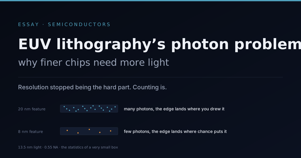
Run the arithmetic on a typical published dose of 30 millijoules per square centimetre. A 20 by 20 nanometre feature receives on the order of eight thousand photons. An 8 by 8 nanometre feature receives around thirteen hundred, and since resists absorb only a fraction of what lands on them, the number of photons that actually deposit energy in that box is a few hundred.
A few hundred is where physics changes character. Photon arrivals are independent random events, so the count in any small box follows a Poisson distribution, and the relative spread of a Poisson count of N is 1 over the square root of N. Three hundred absorbed photons means a spread of about six percent, feature to feature, from nothing but chance. Not a defect in the mask, not a misalignment, not vibration. The same exposure, the same everywhere, and a six percent scatter in how much energy each individual feature received.
Most of that scatter is harmless. It shifts a line width by a fraction of a nanometre and the transistor still works. The tail is what kills you. Somewhere out on the low side of the distribution sits a contact hole that received so few photons that it never opened, and out on the high side a gap between two lines that received so many it closed. These are called stochastic defects, meaning defects with no cause you can find and fix, because the cause is that a fair coin came up heads eleven times. On a chip with tens of billions of features, an event with a probability of one in ten billion is not rare. It is a Tuesday.
Why you cannot simply turn up the light
The obvious fix is more photons: raise the dose, shrink the noise, kill the tail. Every photon you add costs exposure time, and exposure time is throughput, and throughput is the entire economic case for a machine that costs four hundred million dollars.
Resist chemists have spent thirty years on the other end of this, trying to make films that respond to fewer photons. This runs into a wall the field calls the RLS trade off, for resolution, line edge roughness and sensitivity. You can have any two. A resist made more sensitive, so it needs less light, is one in which a single absorbed photon triggers a longer chain of chemistry, and a longer chain travels further from where the photon landed, which blurs the edge. Sharpen the edge by shortening the chain and you need more photons again. Metal oxide resists, which absorb extreme ultraviolet far better than the organic polymers they replace, genuinely move the line, and they are the main reason single exposure printing at a 20 nanometre pitch is possible at all. They do not repeal the trade off.
High NA adds its own bill. Widening the aperture shortens the depth of focus, the vertical range over which the image stays sharp, which falls roughly as the square of the aperture. That forces thinner resist films, and a thinner film absorbs fewer photons, which puts you back in the previous paragraph. The anamorphic optics that make the wide aperture possible also cut the printable field in half, from 26 by 33 millimetres to 26 by 16.5, so large chips must be printed in two halves and stitched, with the stitch itself becoming a place where things go wrong.
Where this stands in 2026
The first commercial High NA machine is now in a factory rather than a laboratory. Intel has installed an ASML TWINSCAN EXE:5200B for its 14A node, with risk production, meaning limited runs used to find out what breaks, expected from 2027. Imec took delivery of its own EXE:5200 in March 2026 for the European pilot line.
TSMC, which manufactures more leading edge silicon than anyone, has said it will not use High NA for its A14 node. Its stated reason is not that the technique fails but that it does not pay: the company judges the tool too expensive relative to printing the same layers with several passes of the older 0.33 aperture machines it already owns. Multiple exposures cost time and stack up alignment errors, but they use paid for equipment. That is a real disagreement about arithmetic between two companies with full access to the same data, and it will not be settled by argument.
Meanwhile ASML is attacking the problem from the source end, where it belongs. The company has demonstrated a thousand watt in band source, up from roughly six hundred watts in today’s best tool, by doubling the tin droplet rate and reshaping the laser pulse train, and projects around 330 wafers per hour by 2030 against roughly 220 now. More power is the one lever that improves resolution, roughness and throughput at the same time, which is exactly why it is the hardest one to pull.
What this does not settle
The imec yield figure is a research result on a test structure, not a product. Test structures are designed to be measurable; real chips have corners, contacts and layers that interact. Wafer throughput, source power and overlay numbers in this piece come from the toolmaker and are specifications rather than independently audited field measurements. The photon counts are an order of magnitude calculation from a nominal published dose, meant to show how the scaling works, not to describe any particular process, which would depend on the specific resist, its absorption and its post exposure chemistry.
And the deeper question is open. Shot noise is not a manufacturing defect that better engineering removes. It is the discreteness of light showing up at a scale where the discreteness matters. Every route past it, more power, better absorbing resists, machine learning that predicts where defects will fall and adjusts the mask to compensate, buys margin against a floor that does not move. At some point the industry stops printing patterns and starts managing a yield distribution, and it is worth noticing that this has already happened.
Further reading
- Imec demonstrates electrical yield for 20 nm pitch metal lines with High NA single patterning, imec press release
- Five things you should know about High NA EUV lithography, ASML, on the anamorphic optics and the half field
- Production of 13.5 nm light with 5 percent conversion efficiency from a laser driven tin microdroplet plasma, Applied Physics Letters
- Tennant’s Law, Chris Mack, on why resolution, roughness and speed refuse to improve together